How Custom CMOS Image Sensors Enable Extreme Low-Light Imaging Applications: Part II
Backside-illuminated CMOS image sensors (BSI-CIS) deliver greater performance than image intensifier (II) and electron-multiplying charge-coupled device (EMCCD) technologies in low-light applications. Developed by Forza and EOTech, these sensors offer excellent low-noise performance thanks to the electron-bombarded semiconductor (EBS) gain process.
In previous blog posts, we discussed the EBS process and how the BSI-CIS meets advanced requirements. For this final installment, we will dive into the design of the MV3.7 BSI-CIS and the electron-bombarded active pixel sensor (EBAPS®). We’ll also take a look at their roles in a low-light camera.
MV3.7 BSI-CIS Architecture
The MV3.7 is a BSI-CIS that was specifically developed to allow the ISIE19 EBAPS® to meet low-light requirements. Compared to the previous generation’s ISIE11 sensor, the MV3.7 features a maximum frame rate of 160 hertz (Hz) and a reduced noise floor, improving detection efficiency for single photoelectrons. This BSI-CIS also features an increased dynamic range of 16 bits, as well as a larger imager format and size of 3.7 megapixels.
Adhering to the standard 110-nanometer design rule, the MV3.7’s 1920 x 1920 active image array consists of 9.117-square-micrometer pixels. To enable off-chip temporal noise correction, the array also features 33 shielded dark columns on either side. Surrounding the array, an additional 15-pixel boundary ensures uniform response.
A lateral integrated capacitor (LOFIC) pixel architecture maintains a linear high dynamic range (HDR). In a LOFIC architecture, the overflow capacitor (OF) retains the charge generated by the photodiode, enabling the capture of fast transient flashes.
At 65ºC, the MV3.7’s EBS gain process ensures minimal dark current noise, allowing the ISIE19 EBAPS to limit dark current from the photocathode at temperatures up to the camera’s maximum operating temperature.
A gallium arsenide (GaAs) photocathode allows the ISIE19 EBAPS to minimize dark current at elevated temperatures. The EBS gain process allows the EBAPS to detect single photoelectrons independent of the MV3.7 frame rate, which is possible due to the ratio between the electron bombarded gain and the CIS noise floor. As the applied voltage between the photocathode and CIS anode increases, the gain also increases.
Figure 1 shows how EBS gain changes with the applied voltage. You can see that the ISIE19 exhibits an EBS gain of around 300 (e-/pe-) at the 1,750-volt operating voltage. At this operating voltage, the MV3.7 has a read noise floor of 5.1 e-.
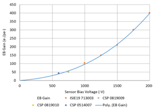
Figure 1: Electron bombarded gain versus voltage.
Figure 2 shows distribution curves of pulse height against applied voltage at a 120-Hz frame rate. As the applied bias voltage increases, photoelectrons strike the anode with higher energy, which generates more electron-hole pairs (EHP) and increases the silicon depth of the generated EHP median.

Figure 2: ISIE19 histograms as a function of voltage.
The ISIE19 and ISIE11 offer different HDR capabilities as shown in Figure 3. In this test, both cameras used the same objective lens while the ISIE19 was set to 120 Hz and the ISIE11 to 60 Hz. Twelve frames of the ISIE19 were averaged while the ISIE11 had six frames averaged to equally represent 0.1 seconds of image capture.
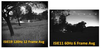
Figure 3: HDR scene comparison between the ISIE19 and the ISIE11.
The Miniaturized Chip-Scale-Packaged (CSP) MV3.7 EBAPS
Some camera applications require image sensors that are more compact than the ISIE19, which is why we designed the chip-scale-packaged (CSP) MV3.7. A standout feature of the CSP is that it does not feature the ceramic package used in the ISIE19. Instead, it forms the photocathode vacuum seal directly with the MV3.7 chip. This miniaturized sensor supports a 25-millimeter-square camera module.
Compact cameras are frequently used in a wide range of applications. One strategy in achieving a small-size camera is to reduce the size of the high-voltage power supply (HVPS) in a camera system. This size reduction can be accomplished by reducing the voltage required to bias the EBAPS photocathode. Because optimal EBAPS performance requires the photoelectron’s electron bombarded gain to greatly exceed the CIS read noise upon impact, the MV3.7’s read noise of roughly 5.1 e- made it ideal for the CSP prototype.
Thanks to the EBS process, a custom BSI-CIS like the MV3.7 can enable the ISIE19 EBAPS to deliver excellent low-light camera performance. Contact us to learn more or read our white paper.